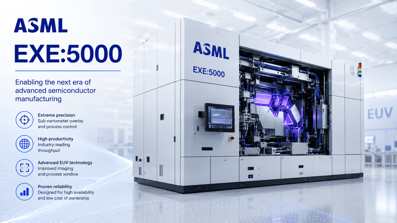
ASML EXE:5000 brings 0.55 NA High-NA EUV to advanced chip manufacturing
ASML’s TWINSCAN EXE:5000 is the first generation of the company’s High Numerical Aperture extreme ultraviolet lithography, or High-NA EUV, platform. It increases numerical aperture from 0.33 on ASML’s established NXE EUV machines to 0.55, reducing single-exposure resolution from about 13nm to 8nm.
That change gives semiconductor manufacturers another route to producing increasingly dense logic and memory chips without relying as heavily on double or triple patterning. ASML positions the EXE platform for advanced logic beginning around the 2nm generation and for leading-edge memory at similar transistor densities.
The EXE:5000 itself is best understood as the first-generation High-NA development and qualification platform. ASML shipped its fifth and final EXE:5000 during the first quarter of 2025 before moving to the faster EXE:5200B for production-oriented deployments.
Why High-NA EUV matters
Lithography systems project extremely small circuit patterns onto light-sensitive material covering a silicon wafer. The minimum feature size they can resolve depends partly on the wavelength of the light and the numerical aperture of the projection optics.
ASML expresses this relationship through the Rayleigh criterion:
CD = k₁ × λ / NA
CD represents the critical dimension, λ the wavelength and NA the numerical aperture. Increasing NA therefore allows a lithography system to resolve smaller features without changing the wavelength.
ASML’s conventional NXE EUV systems already use extremely short 13.5nm EUV light, compared with 193nm for high-resolution ArF deep-ultraviolet lithography. The EXE generation keeps the 13.5nm wavelength but increases the numerical aperture from 0.33 to 0.55.
That takes ASML’s stated single-exposure resolution from approximately 13nm to 8nm.
8nm resolution does not mean an 8nm processor
The 8nm figure can be confusing because ASML also positions High-NA EUV for 2nm-class semiconductor processes.
These numbers describe different things.
ASML’s 8nm specification is the lithography system’s critical-dimension resolution. Process names such as 2nm, Intel 18A or future angstrom-class nodes identify semiconductor technology generations. Modern process-node names no longer correspond directly to one physical transistor measurement.
An EXE:5000 can therefore provide 8nm lithographic resolution while helping manufacture chips belonging to a nominal 2nm process generation. ASML says High-NA EUV is intended to support advanced logic beginning around the 2nm generation, followed by memory processes at comparable transistor densities.
Larger optics raise numerical aperture to 0.55
The EXE:5000’s defining hardware change is its projection-optics system.
Higher numerical aperture requires larger mirrors. EUV lithography cannot use conventional glass lenses because most materials absorb 13.5nm light, so ASML and its optics partner ZEISS rely on extremely smooth multilayer mirrors operating inside a vacuum. ASML says its EUV mirrors contain more than 100 engineered material layers.
Simply increasing mirror size created another problem. Light would strike the reticle at a greater angle, reducing its reflectivity.
ASML and ZEISS addressed this with anamorphic optics. Instead of reducing the reticle pattern equally in both directions, the EXE system demagnifies it by 4× in one direction and 8× in the other. This allows High-NA imaging while retaining the semiconductor industry’s established reticle format.
It is similar in principle to anamorphic optics used in cinematography, where an image is compressed differently across two axes.
The trade-off is a smaller exposure field
Anamorphic imaging introduces its own consequence: the EXE platform exposes only half the field area of an NXE system in each shot.
That means the scanner must perform roughly twice as many exposures to cover the same wafer area. ASML therefore had to redesign the motion systems to move substantially faster.
The EXE wafer stage can accelerate at 8g, twice the rate of an NXE wafer stage. Its reticle stage reaches 32g, four times the corresponding NXE system.
For very large chip designs that exceed a High-NA exposure field, manufacturers can also use stitching. The system exposes adjacent fields that form a larger design.
ASML’s February 2026 roadmap distinguishes throughput with and without stitching, showing that stitching carries a productivity penalty.
EXE:5000 reaches 110 wafers per hour at a 50mJ dose
ASML’s current roadmap specifies the EXE:5000 at 110 wafers per hour without stitching and 75 wafers per hour with stitching, based on a 50mJ/cm² exposure dose.
The same roadmap lists matched-machine overlay at 1.1nm or better.
Earlier ASML material quoted more than 185 wafers per hour for the EXE:5000, but throughput figures depend heavily on exposure dose and test conditions. ASML’s newer 2026 roadmap provides the more useful comparison because it specifies the 50mJ/cm² condition and separately identifies stitched operation.
ASML EXE:5000 specifications
| Specification | ASML TWINSCAN EXE:5000 |
|---|---|
| Product type | High-NA EUV lithography system |
| EUV wavelength | 13.5nm |
| Numerical aperture | 0.55 NA |
| Resolution | 8nm |
| Previous EUV generation | 0.33 NA NXE |
| Imaging contrast | About 40% higher than NXE |
| Projection design | Anamorphic reflective optics |
| Demagnification | 4× in one axis, 8× in the other |
| Exposure field | Half the area of NXE per exposure |
| Throughput without stitching | 110 wafers/hour |
| Throughput with stitching | 75 wafers/hour |
| Throughput reference dose | 50mJ/cm² |
| Matched-machine overlay | ≤1.1nm |
| Wafer-stage acceleration | 8g |
| Reticle-stage acceleration | 32g |
| Main target | Advanced logic and memory |
| Starting logic generation | Around 2nm class |
| Successor | TWINSCAN EXE:5200B |
ASML states that High-NA provides approximately 40% greater imaging contrast than its NXE platform. Better contrast can improve pattern definition and potentially allow a lower exposure dose for some layers.
How the EXE:5000 creates EUV light
High-NA changes the optics, but the EXE platform retains the fundamental EUV light-generation approach developed for ASML’s NXE systems.
The source fires laser pulses at microscopic droplets of molten tin travelling through a vacuum. An initial pulse reshapes the droplet, while a more powerful pulse turns it into a plasma that emits 13.5nm EUV radiation. ASML says this process occurs tens of thousands of times every second.
A collector mirror captures the resulting EUV light and directs it through the illumination and projection system.
Because EUV is readily absorbed by most materials, the complete optical path depends on reflective mirrors and vacuum conditions rather than conventional transmissive lenses.
This complexity is one reason an EUV scanner should not be thought of as merely an unusually powerful camera. It combines plasma physics, lasers, vacuum systems, advanced optics, nanometre-scale positioning, sensors and computational correction into one manufacturing platform.
High-NA can reduce multiple patterning
The principal manufacturing argument for High-NA is not just that it can print smaller structures. It can potentially print some structures in one exposure that would require several patterning steps using lower-resolution equipment.
Multiple patterning allows chipmakers to extend an existing lithography system beyond what it can resolve directly. However, each additional patterning step adds masks, deposition or etch operations, wafer handling and opportunities for alignment errors.
ASML says moving selected layers from double or triple patterning to single High-NA exposure can reduce manufacturing complexity, cycle time and defect risk.
This does not mean every lithography layer on a future chip will move to High-NA.
Chipmakers choose lithography equipment layer by layer according to resolution, manufacturing cost and yield. Older DUV equipment, 0.33 NA EUV and High-NA EUV can therefore operate alongside one another in the same advanced fab.
ASML demonstrated 10nm dense lines in 2024
The EXE:5000 initially served as a development system for the semiconductor ecosystem.
ASML and imec opened a joint High-NA EUV Lithography Lab in Veldhoven in June 2024. The facility gives logic and memory manufacturers, material companies and equipment suppliers access to the EXE:5000 alongside resist-processing, metrology, mask-handling and inspection equipment.
During early commissioning, the platform produced 10nm dense lines with a 20nm pitch on metal-oxide resist. ASML noted that the scanner had only completed coarse calibration at that stage, so the demonstration did not represent its full production performance.
This type of development work is essential because introducing a new lithography platform affects far more than the scanner itself.
Chipmakers also need compatible photoresists, masks, computational lithography, inspection, metrology and etch processes.
Intel received the first commercial EXE:5000
ASML shipped the first modules of the first customer EXE:5000 to Intel in December 2023. Intel subsequently assembled the system at its D1X research fab in Hillsboro, Oregon.
Intel describes the installed High-NA system as weighing about 165 tonnes and being roughly comparable in size to a double-decker bus. The EXE:5000 reached Oregon in more than 250 crates packed into 43 freight containers.
By the first quarter of 2025, ASML had shipped its fifth and final EXE:5000, with systems placed at three customers. The company then transitioned new High-NA shipments to the EXE:5200 generation.
The limited number reinforces the EXE:5000’s role: it established the High-NA platform and allowed leading chipmakers to develop manufacturing processes before wider production deployment.
High-NA has now reached real chip production
The broader High-NA programme has moved substantially beyond laboratory development since the EXE:5000 first shipped.
By the end of 2025, ASML said customers had processed more than 400,000 wafers across High-NA systems, while the company had demonstrated a full-specification EXE:5200B at a customer site.
A more important milestone arrived in July 2026. ASML announced that Intel Foundry had entered high-volume manufacturing for a subset of Core Ultra Series 3, code-named Panther Lake, with selected Intel 18A layers dual-qualified for High-NA EUV at its Oregon operation. ASML said product using those layers was shipping at yields matched to its established NXE platform.
That announcement concerns the EXE High-NA platform, rather than proving that every Panther Lake wafer or every Intel 18A layer uses an EXE:5000 specifically.
High-NA remains a selective manufacturing tool for critical layers.
EXE:5200B is the production-focused successor
The EXE:5200B retains the same 0.55 NA and 8nm resolution while increasing throughput and improving overlay performance.
ASML’s 2026 roadmap lists it at 175 wafers per hour without stitching and 135 with stitching, again at 50mJ/cm². Matched-machine overlay improves to 0.8nm or better.
ASML says the 175-wafers-per-hour figure represents a 60% productivity improvement over the EXE:5000. The gain comes partly from an improved EUV source delivering more power at wafer level, while updated ZEISS optics reduce aberrations and improve imaging and overlay.
This distinction matters when evaluating the EXE:5000 in 2026. The 5000 established High-NA technology, while the 5200B takes that architecture towards larger-scale manufacturing.
Where will the EXE platform be used?
Advanced logic processors
ASML originally positioned the EXE platform for logic processes beginning around the 2nm generation.
The most advanced CPUs, GPUs, AI accelerators and mobile processors contain extremely dense critical layers where reducing multiple patterning can offer manufacturing benefits.
Intel’s 2026 use of High-NA on selected 18A layers provides the first publicly confirmed high-volume logic example.
DRAM manufacturing
ASML also targets leading-edge memory.
DRAM manufacturers continually shrink the structures used to create memory cells while increasing density. High-NA’s greater resolution can help print future critical memory layers with fewer patterning steps.
Semiconductor process research
The EXE:5000 has been particularly important as an R&D platform.
Manufacturers can use it to develop photoresists, masks, etch processes and device layouts years before a full High-NA process enters mass production. The ASML-imec lab was created specifically to give the wider semiconductor ecosystem access to that development environment.
AI and high-performance computing
The scanner does not perform AI computation itself, but it enables the fabrication techniques needed for increasingly dense processors.
ASML identifies AI-related demand as an important driver of leading-edge logic and memory investment. High-NA can therefore influence future AI accelerators indirectly by enabling manufacturers to place more advanced structures on their silicon.
High-NA also creates new manufacturing challenges
Higher resolution is not free.
The smaller exposure field creates potential stitching requirements for large dies. The reduced depth of focus associated with higher NA also increases demands on wafer flatness, process control and focus accuracy.
Chipmakers additionally need new resist processes, mask strategies, metrology and inspection techniques. ASML and imec began preparing this supporting ecosystem years before the first EXE:5000 became operational.
High-NA therefore competes not only on whether it can print a smaller feature, but on whether doing so delivers a better manufacturing cost and yield than extending conventional EUV through multiple patterning.
Different semiconductor manufacturers may consequently introduce High-NA at different nodes and on different numbers of layers.
What the EXE:5000 means for South African technology users
The EXE:5000 is specialised semiconductor-fabrication infrastructure rather than equipment that normal South African companies would deploy.
Its impact will arrive indirectly.
Future processors manufactured with High-NA could appear in notebooks, smartphones, servers, AI accelerators and cloud infrastructure used by South African consumers and organisations.
The important point is that High-NA does not automatically make a processor faster. ASML provides the manufacturing capability. The eventual processor architecture, transistor design, power limits, packaging and software determine what a finished product can actually do.
Why the ASML EXE:5000 matters
The EXE:5000 marks the largest optical change to production-oriented EUV lithography since ASML introduced the NXE platform.
Moving from 0.33 to 0.55 NA reduces ASML’s single-exposure resolution from about 13nm to 8nm. Anamorphic optics, faster stages and greater imaging contrast allow chipmakers to consider replacing some complicated multi-patterning flows with single High-NA exposures.
The EXE:5000 itself will not be ASML’s main volume-production machine. Its successor, the EXE:5200B, provides substantially higher throughput and better overlay.
Its historical and technological importance is nevertheless considerable. The EXE:5000 took High-NA EUV from years of optical research into working customer fabs, and the platform it established has now reached its first high-volume logic products.


