ASML: the machines that print patterns for semiconductor manufacturers
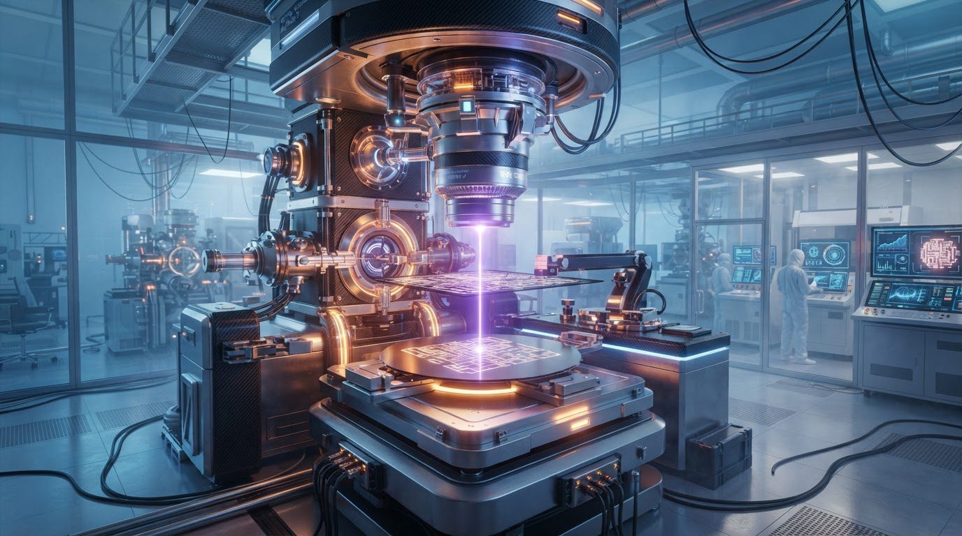
ASML builds lithography systems used in chip manufacturing. Its equipment helps transfer patterns onto silicon wafers, supporting the repeated, precise steps needed to form semiconductor circuits.
The company supplies the tools used by chipmakers. It should not be described as a retail processor brand or as the manufacturer of every finished chip made with its equipment.
A venture created by Philips and ASMI
ASML’s history begins in 1984, when Philips and Advanced Semiconductor Materials International created ASM Lithography. The company initially worked from a building near Philips in Eindhoven.
It moved to Veldhoven in 1985 and became an independent publicly listed company in 1995. These corporate origins are more precise than attributing the business to an invented individual founder.
The company overview describes hardware, software and services for semiconductor production. That breadth reflects the fact that a lithography machine must work within a controlled manufacturing environment, not simply expose one isolated image.
What lithography contributes
A semiconductor design has to become a physical pattern on a wafer. Lithography uses light to expose selected patterns during the manufacturing process.
The useful distinction is between designing the circuit and reproducing the required patterns. The machine contributes precision and process capability, while the customer’s design and wider fabrication steps determine the finished product.
A highly capable exposure system therefore cannot, on its own, establish the speed of a processor or the yield of an entire factory. Those are outcomes of a larger process involving many interdependent steps.
EUV and DUV are not a simple old-versus-new choice
ASML’s product portfolio includes extreme ultraviolet and deep ultraviolet lithography systems. EUV attracts attention because of its role in demanding patterning requirements, but DUV remains part of semiconductor manufacturing.
The company’s DUV explanation notes that a chip can use different lithography technologies for different layers. A more demanding layer and a less demanding layer do not necessarily call for the same exposure method.
That matters when interpreting equipment investment. The presence of DUV does not automatically make a production line obsolete, and an EUV machine does not mean that every layer or every other manufacturing step uses the same technology.
Software and measurement close the loop
Computational lithography, metrology and inspection sit alongside the exposure systems. Modelling helps prepare and optimise patterns, while measurement and inspection help establish what the process actually produced.
The relationship is a feedback loop between the intended design and the manufactured result. Precision in one step has to be maintained across the process; an error cannot be understood solely by looking at the machine’s headline specification.
This also gives software a direct manufacturing role. It is part of preparing and controlling the process, rather than an unrelated office application attached to a hardware business.
Installed systems have an operating lifecycle
ASML also offers refurbished systems and customer support. Equipment continues to need maintenance, upgrades and process integration after its original delivery.
A factory purchase is consequently different from buying a standalone consumer device. The customer’s production requirements and the support of an installed fleet matter alongside a new system’s capabilities.
ASML’s position in technology comes from this specialised role in patterning. Understanding the distinction between the toolmaker, the chip manufacturer and the chip designer makes semiconductor announcements much easier to assess.